single-ended buffer (SE-buffer)
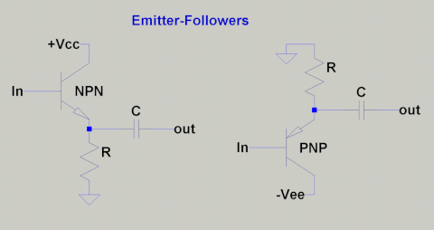
The simplest form of a SE-buffer is the emitter-follower, working upon a resistor as load. The signal is taken AC-coupled from the output through Capacitor C.
By action of the base voltage and the emitter resistor a bias current flows, that needs to be larger than the maximal expected load currrent into a attached external load.
The voltage gain is close to 1 (typically between 0.95-0.99).
The distortion level is just mediocre, but sufficiently low enough for Audio useage.
A big disadvantage is the low efficiency which may reach 12.5% at best.
Efficiency may be doubled up to 25% if a current source is used instead of the simple loading resistor. The current source may be made from a true active current source or a accordingly valued inductance.
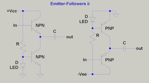
The current source enhances the circuits linearty. Reduced distortion, lower output impedance, and a up to 25% raised efficiency are the result of only a few parts more. The gain is a bit closer to 1. The circuit can be used for good in line-level circuits in preamplifiers or filters.
It not only suffices technically but most often it sounds more pleasant than OP-Amp circuits.
As one can see from the Figures the circuit may be used with a single voltage rail or dual-symmetric supplies. If the transistors are well matched and with precise trimming one can omit with the output coupling cap alltogether.
Used in preamps or filters the low efficiency doesn´t normally play a role.
To drive headphones or even loudseakers properly a higher efficiency is desirable.
To achieve higher efficiency either the loading constant current source needs to be modulated and/or we have to switch from class-A to class-AB.
The latter is easily possible using complementary transistors.
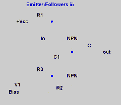
The circuit in Fig.3 is still a SE-emitter-follower, but its midway to a PP-buffer, because the loading resistor is replaced by a modulated current source instead.
Functioning:
DC-wise the capacitor C1 is a open. The ´lower´ NPN transistor receives a constant bias voltage via R2/R3. As such it works as a constant current source towards the ´upper´ NPN transistor.
Under AC-conditions C1 becomes a short and the signal-dependent voltage drop over R1 superimposes the DC-bias voltage at the ´lower´ NPNs base.
The current source is now modulated, depending on the audio signal.
As the ´upper´ NPNs collector voltage is out of phase (inverting), the current source is modulated the same inverted phase, hence it works in opposition to the ´upper´ NPNs emitter current.
We find a push-pull action here but with same gender transistors.
The maximum current into a attached load may reach twice the bias current value.
The circuit requires class-A biasing.
The maximum efficiency may reach 50%.
push-pull buffer (PP-buffer)
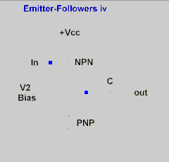
The useage of complementary transistor types like shown in Fig.4 is more elegant.
Biased in class-A the same applies for the maximum load current and efficiency as for the circuit of Fig.3. The complementary circuit can also work in class-B mode.
In this mode one transistor cuts off over one half of the signal-cycle.
The cut-off and turn-on action of the two partners never happens in perfect synchronocity and mirror-image like.
This leads to crossover- and switching-distortions, forms of distortion that negative feedback can´t correct for.
The efficiency may be even higher than 70% though.
Typically a complementary stage is used with dual symmetrical supply rails. The complementary emitter-follower is the workhorse of probabely 95% of all power amplifiers.
Diamond-structure
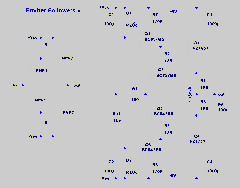
The generation of the required biasing voltage for power amplifiers is no trivial task at all. At line-level it is though. A quite felicitous exmple is the so called Diamond buffer.
Principally the Diamond is a series connection of two complementary emitter follower pairs.
See Fig.5 left side, principle schematic.
The forward voltage of the Vbe path of the input transistors functions as bias voltage generator for the output transistors.
The resistors function as current paths for the input emitters and as a supply for the required base current of the output emitter-followers.
Ideally the Rs would be replaced by constant current sources, because the sensitivity against noise and spikes on the supply rails would become very low.
The PSRR (Power Supply Rejection Ratio) becomes large
The right hand side of Fig.5 presents a completely dimensioned circuit fed from +-9V supply rails.
We recognize Q1 and Q4, resp. Q2 and Q3 as the two NPN-PNP emitter-follower pairs. Resistors R2, R3 generate enough bias voltage such that the transistors Q3 and Q4, inclusive the voltage drop over their emitter resistors R4 and R5, are turned on surely.
Q1s and Q2s collectors are not connected to te opposite side supply rail but to the opposite sides emitter resistors.
Besides reducing the heat power losses of Q1 and Q2 considerably, this trick reduces distortion due to local feedback loop action.
The current sources (Rs in the left handed principle schematic of Fig.5) are replaced by much more stable transistorized current sources made from Q4/R7/D1/C1 and Q6/R8/D2/C2.
The red LEDs D1 and D2 have a very constant forward voltage due to their high delta-current-to-delta-voltage ratio. They are excellent reference voltage devices for constnat current sources. Thermal drift compensation may be achieved by close thermal coupling of the LED and the transistor.
The anyhow lownoise LEDs are further de-noised and stabilized by Caps C1 and C2.
The emitter resistors R4 and R5 (as well as R2 and R3) linearize the transistor curves and reduce tolerance sensitivity of the circuit against varying transistor parameters.
C3 and C4 serve as local energy reservoirs.
Q1 to Q4 are BC847BS and BC857BS, dual matched transistors manufactured by Diodes (Zetex). They are SMD variants of the well known BC550/BC560 (TO92).
Alternatives are the single BC327/BC337 in TO92 casing, resp. BC807/BC817 in SOT23 SMD casing (also BC807DS/BC817DS as duals in SOT457 SMD casings).
A bit more exotic are the THAT340, lownoise quads from That Corp. that contain 2 matched NPN and PNP pairs each in a single casing (SO14).
Also from Zetex come the output transistors FZT651/FZT751 in SOT223 SMD casing.
These have to deal with considerable amounts of heat power losses and require sufficient cooling with heat sinks.
Very good throughhole alternatives would be the Toshiba 2SA1015/2SC1815 in TO92 casing or the even more beefy Hitachi 2SB649/2SD669 in TO126 casing.
For slightly lower requirements the good old BD139/BD10 will do fine.
This simple circuit measures excellent.
All parameters are unobjectionably low, even close to traceablity.
The circuit can easily be modified for higher supply rails or different power requirements.
It useable as line-level preamplifier, or headphone-amp and even small power amplifier.
Sonically the low parts number count pays off, compared to OP-Amps.
Current Mirror assisted Buffer
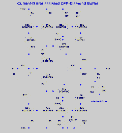
The circuit can be pimped to achieve better PSRR by implementing current mirrors that block against the supply rails.
One recognizes the diamond structure made up from transistor-pairs Q1a/Q2b and Q1b/Q2a.The CFP-structure can be recognized from Q2b/Q7 and Q1b/Q8. Q3a/Q3b and Q4a/Q4b are current mirrors working as constant current sources for the input transistors. They themselves are supplied by a degenerated JFET constant current source built from J1/R14. Instead of J1/R14 a simple high-ohmic resistor suffices, reducing cost and easing sourcing.
Q5a/Q5b and Q6a/Q6b also form current mirrors. In this case though the two legs run at different idle current values, which are scaled by differing emitter resistors. R9 in parallel to the Poti allows for sensitive trimming of the output offset voltage. Fully DC-coupled action is possible.
One may use lowlevel transistors, prefferably dual types. Good functioning of the current mirrors is guaranteed by tight matching and close thermal contact of the two transistor-dies within the same casing.
Even if the currents in the output legs are high, lowlevel transistors still suffice, due to the low collector-emitter voltages and hence low heat power losses. The headroom is only slightly reduced, approximately 1.5V below the supply rails. Because of the current mirrors much higher output impedance compared to emitter resistors alone, the compensation capacitors can be chosen smaller in value, which also reduces distortion a bit. All in all the circuit has reduced requirements regarding the quality of the power supplies.
Even if 14pcs. (15pcs J1 included) of transistors are required the PCB may still be very compact if dual SMD transistors are used.
The SOT363 casings for Q1-Q6 measure max. 2.2x2.2mm. The SOT23 for J1 measures ca.3x2.3mm.
The SOT223 of Q7 and Q8 are a bit bigger at 6.5x7mm and require a few cm² PCB copper area as cooling fin.
A DC-Servo circuit that keeps the output offset voltage under all circumstances at 0V is also easy to implement. Quite often one can find DC-servos that feed the corrective signal directly into the input of the circut. Besides the inevitable noise there remain signal artefacts left from far up in the audio frequency range. A classic amplifier or buffer of OPamp style would amplify these artefacts initially with its full openloop gain. Sonic penalties can´t be avoided this way.
I regard it to be better to feed the DC-correction signal into a node that reacts much less sensitive. Similar to the fixed trimming through Poti P1, the DC-servo signal could for example be fed to a emitter of the current mirror transistors Q3 or Q4. A OPAmp, referenced to 0V could steer a transistor that translates the corrective voltage into a corrective current and that translates the level from 0V towards the emitter-potential at the same.
Bootstrapped Buffer
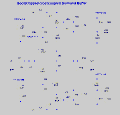
The circuit of Fig.7 is simpler again but achieves very low THD through bootstrapping. In this case bootstrapping is achieved in that the bases of Q5 and Q6 track the voltage of the node R7/8/16/16 by a constant voltage value above, resp. below. Since the Vbe of the transistors Q5 and Q6 changes only a few mV even for large collector current changes the emitters also track the output voltage. At the same this means that the collector-emitter voltages of the four transistors Q1-Q4 remain almost constant. In addition the voltages over R5 und R6 vary by only a few mVs, instead of the usual full signal voltage stroke. The resistance value is increased dynamically multiple times. this works so well that nearly the same results as if using a true JFET current source can be achieved.
A 22k resistor could be raised to more than 1MOhm dynamically. Results are even better with the JFET in place, because that´s impedance can be well up in the lower MOhm range already without bootstraping. Using them costs on headroom though since their drain-source voltage must be subtracted ... and the Vds should not be lower than twice the gate-source voltage of the JFET. One could circumvent this problem by routing the JFET current sources not to the emitters of Q5/Q6 but to the supply rails.
Would You route the resistors to the rails instead You´d loose the dynamic resistance increasing effect which would immidiately lead to increased distortions.
Die Nutzung der Texte, Bilder und Informationen auf dieser Webseite in Teil oder in Gänze bedarf meiner Zustimmung. The useage of the texts, pictures and information contained on this website in parts or in fullness requires my admittance.
Diese Webseite wurde mit Jimdo erstellt! Jetzt kostenlos registrieren auf https://de.jimdo.com
