hybrid-buffer
As written in the chapter about transistors hybrid circuits are defined as a combination of differing active devices, for example tubes and transistors, bipolars and MOSFETs or JFETs.
This aims to combine the positive properties of the devices and to eliminate their negative properties. In the first instance I´d lke to discuss buffers that make use of JFETs, MOSFETS and bipolars.
(cascoded) hybrid-Darlington buffer

The problems of the simple JFET-buffers in driving into low-impedance loads can be circumvented with a little more effort, in that more transistors are used that deliver the additional current.
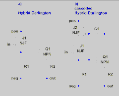
In circuit a) the JFET is working in source-follower mode. Its source current generates a voltage drop over resistor R1, that at the same is the base voltage of the bipolar transistor Q1. With sufficiently large voltage drop Q1 opens up and its emitter current adds to the JFETs source current at the output node ´out´. The emitter resistor R2 defines the part of current through Q1 and reduces its tolerance sensitity.
The circuit allows for the use of high-ohmic source resistors for the JFETs, thereby reducing the effects of the typically large tolerances.
The bipolar Q1 takes on most of the current and provides for a low output impedance. J1 can therefore be a high-gm lowlevel JFET, for example a 2N/MMBF/SST 4393 or 4392. It only must be ensured that its gate-source voltage at the working point is higher than the approximately 700mV the bipolar transistor requires as base-emitter voltage.
This rather excludes popular JFETs like 2SK170 or BF862 from the list, resp. proper candidates have to be chosen carefully by screening.
The circuit at b) expands the first one in that the JFET J1 is cascoded by a second JFET.
Here J2s gate-source voltage is J1s drain source voltage at the same.
The current flowing through J1 and J2 is identical (neglecting gate leakage).
Due to J2s transconductance its gate-source voltage hardly varies with varying drain current.
This means, that J1 works under nearly constant drain-source voltage condition.
This leads to drastically reduced distortion and J2 takes over a major part of the heat power losses from J1. J2s gate-source voltage at the working pont should exceed >>2V to ensure that J1 stays in the linear part of its Id-Vds curve. A suitable candidate is the 2N/MMBF/SST 4391.
The headroom of the circuit reduces though, because J2´s drain-source voltage needs to be subtracted from the rail.
Also, there is a possibility for oscillations, which may require capacitor C1 for compensation.

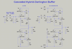
A completely dimensioned circuit is shown in Fig.2.
One can easly identify a upper part and a nearly identical lower part. The upper part can be viewed as the signal-part, while the lower part forms a current source load. In a) the current source is of constant type, while in b) its a modulated source.
Variant b) has the advantage that it can push a higher maximum current into a attached external load, or the external load may be much lower in impedance.
Resistor R9 is wired in series to the upper part of the buffer´s supply rail.
The voltage drop over R9 is proportional to the current flowing through it (hence the current flowing through the upper buffer part), which is the sum of the DC-idle current and the audio signal related AC-current.
The voltage at node ´mo´ is AC-coupled (free of DC) to the gate of the current source part.
It modulates the current source in a opposing way to the upper part, hence the circuit functions in push-pull.
Resistor R10 serves to create the same rail conditions in the lower part of the circuit as occur in the upper branch.
Without R10 the heat power losses of J4 and Q2 would differ from and be higher than those of J3 and Q1.
These basic circuits may be varied in that the N-channel-NPN-Darlington is replaced by a complementary N-channel-PNP-Darlington.
This then leads us to the:
hybrid-compound buffer

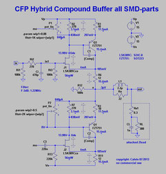
The hybrid-compound buffer is quite similar to the hybrid-darlington buffer from Fig.1a. Its just that the Bases of the bipolar slaves are not connected to the Sources of the associated Master-JFETs, but to their Drains. The bipolar Slaves are of complementary type, PNPs.
The Source resistor also changes its position to the JFET´s Drain. The voltage drop over the Drain-resistor steers the bipolar Slave open. A almost identical hybrid-compound transistor forms the ´negative´ part of the circuit, the current source.
It is modulated for increased current capability via the tap-point ´mo´. The degree of modulaton depends on the tap-point of poti P1 and the attached load impedance. The current amplitude rises with lower load-impedance. The correct value is set in that the lowest-to-expect load impedance is connected to the output and a sine signal is fed into the input.
The current amplitudes through R6 and R11 are then trimmed to best symmetry by P1.
The modulation degree can be set to a fixed value by omitting with P1 and changing R2 to 220Ohms. This makes sense for high-impedance loads.
What differences apply to the compound circuit?
- The JFETs can be lower Idss types (audio-types)
- A hybrid super transistor is formed due to the short and snappy feedback loop. It offers very high input-impedance, very low output-impedance, high current capability and extremely low distortion levels. The compound works very linear because of the very small current amplitudes through the Master-JFET.
- The clipping limit almost reaches to the supply lines. On the other hand one can decrease the supply voltages to keep heat power losses lower. The circuit in Fig.3 can be suppled from +-9V without any issues.
- Because the amplitude of the Drain voltage is large one needs to restrict the supply voltages to rather low levels with many ´Audio-JFETs´ anyway. An eye must be kept on the heat power losses. Also there´s the danger of latch-up due to upshooting Gate-leakage, that occurs under the conditions of high Drain-Source voltage, high Drain current and high temperature.
hybrid-compound-super-buffer or Calvin-buffer

The hybrid compound super buffer expands the hybrid-compound circuit by another cascoding JFET. As such it forms a Sziklai pair in which the steering transistor is replaced by the JFET cascode. The cascode keeps the Drain-Source voltage of the Master-transistor on a almost constant and low level. The advantage is that the Master-JFET works under close-to-constant-voltage- and close-to-constant-current conditions.
The resulting differences are:
- Even lower distortions working under low load-impedances.
- The Master-JFETs can be of low maximum Drain-Gate-, resp. low Drain-Source voltage types
- lower danger of latch-up
- the clipping limit is lower by ca. double the Gate-Source voltage of the cascoding JFET. Actually it doesn´t clip hard but distortions rise considerably. Clipping occurs at approximately Vsupply minus Vgs of the cascoding JFET.
The Hesener-Paradise variant was developed as a spin-off of the original to pimp the existing buffer of the Paradise phono stage designed by Joachim Gerhard.
The Paradise´s buffer was made from a already very good JFET-cascode.
The degree of modulation is fixed in the Hesener-Paradise variant.
In the following my buffer got named Calvin-buffer and it seemingly pleased everybody who switched over from the orignal cascode.
In the meantime the Calvin-buffer became a quite successful build- and group-buy project with over 1.000 PCB-kits distributed.
The original thread can be found at DIY-Audio Forum under the title "Preamp-Buffers - simple idea" at http://www.diyaudio.com/forums/analog-line-level/226099-preamp-buffers-simple-idea.html
Calvin-Buffer plus dc-servo

The output Offset in the above shown "Calvin-Buffer" can be nulled by adjusting R8b in the Hesener-Paradise variant and with P2 in the original.
That allows us to omit with the output coupling cap, with its sometimes quite large capacitance if lowohmic loads like headphones or even loudspeakers need to be driven.
On demand of ac-coupling one may use a input coupling cap with a lower capacitance value (>100nF) due to the high input impedance. The cap may be a compact high-quality yet still lowcost film type.
The adjustment via poti works flawlessly but it remains fixed. Offsets stemming from varying temperature or ageing won´t be corrected for. This requires either a coupling cap or an active dc-servo. Most servos are connected as first grade integrators (-6dB/oct) feeding a corrective voltage back into a input of the circuit.
The servo here works different in that it corrects for the idle current of the Buffer.
It works like this:
Without the servo the upper and lower part of the Buffer circuit are the same, and therefore R7 and R12 are the same. These two resistors define the idle current through the circuit.
With the servo included we choose R12 smaller in value than R7. A larger idle current then flows through the lower part generating a negative Offset at the output, respective at node ´dc´.
Now Q3 and the servo come into the play.
Let us assume that the basis of Q3 finds itself on 0V potential. As its emitter is connected to the positive supply line through R20, Q3 opens up and a current flows from the negative supply line through R12, R21, Q3 and R20 to the positive supply line. The current from the negative supply line splits into two parts, one trough the lower buffer part and the second through Q3. Now it must be made sure that the voltage drop over R12 due to the higher current is exactly the same as the drop over R7. This can be achieved by choosing the value of R20 appropriately.
Now the servo springs into action.
Lets assume a negative offset at the circuit node ´dc´ due to a too high current through the lower Buffer part. This will lead to a negative Offset at the output of the Servo OPAmp (at R19), because it is connected in a noninverting configuration.
This will drive the basis of Q3 more negative and opens up Q3 more. The current through R12, R21, Q3 and R20 grows. The voltage drop over R12 rises too, through which J2, the controlling transistor of the Buffer, closes down, thereby reducing the current through the lower Buffer part. The mean of the Offset voltage at node ´dc´ sinks.
With an positive Offset the servo action is reversed.
A corrective variance around 10% of the idle current value will probabely be sufficient.
This suggest a reduction of R12 by 10% also.
The schematic lists current values of 49mA through R7 and 54mA through R12.
The servo will take on the difference of 5mA. All in all the servo can correct for +-5mA around the idle value of 5mA, hence from 0-10mA.
This would even be sufficient -if both Buffer parts are otherwise identical- to correct for an Offset voltage of +-20mV at the Input, allowing to omit with an input coupling cap also.
A further advantage can be seen in the fact that instead of the usual superposition of the signal voltage with the corrective voltage of the servo, it controls the offset by acting on the idle current directly.
As such it is rather not a part of the direct signal path.
The servo corrects the more sensitive the higher its gain is. At dc it works under openloop condition, meaning with anyway very high gain. Q3 functions as a gain stage also, so that their gains multiply.
This way the servo achieves a very high sensitivy and precision.
Its a bit surprising that this dc-servo is so seldomly used in other circuits.
Die Nutzung der Texte, Bilder und Informationen auf dieser Webseite in Teil oder in Gänze bedarf meiner Zustimmung. The useage of the texts, pictures and information contained on this website in parts or in fullness requires my admittance.
Diese Webseite wurde mit Jimdo erstellt! Jetzt kostenlos registrieren auf https://de.jimdo.com
