L12-2, powerful, good, low-cost
Already a couple of years ago I came across a nice little amplifier of chinese origin on ebay, the L12-2 made by LJM. Its an amplifier designed after the LIN-topology, but it contains a few specialties, that are worth to talk about.
Unfortunately there are quite a number of copies and plagiats around that neither reach the niveau nor tequalities of the original.
The original LJMs show their Logo imprinted on the PCB.
It should be safe to order originals via LJMs shop at the TaoBao platform.
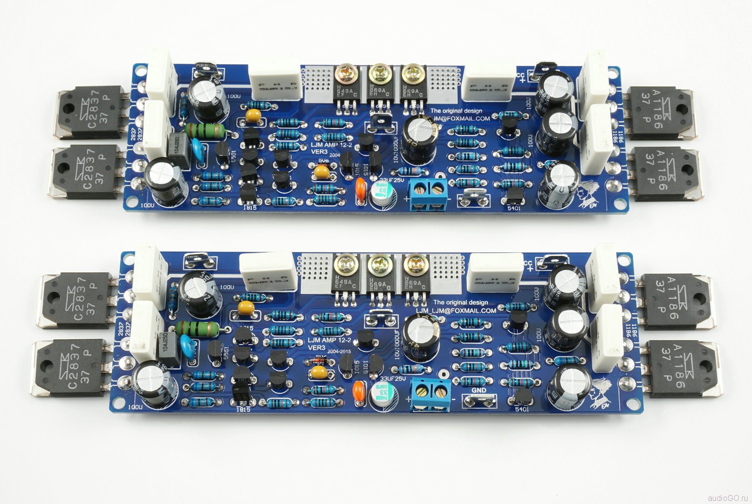
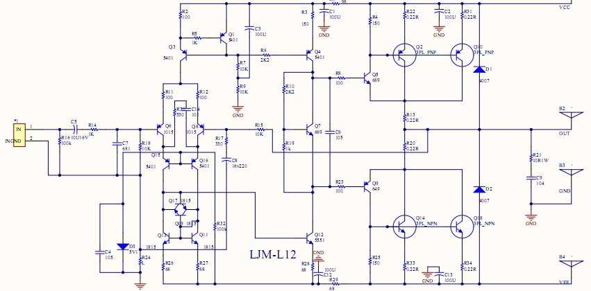
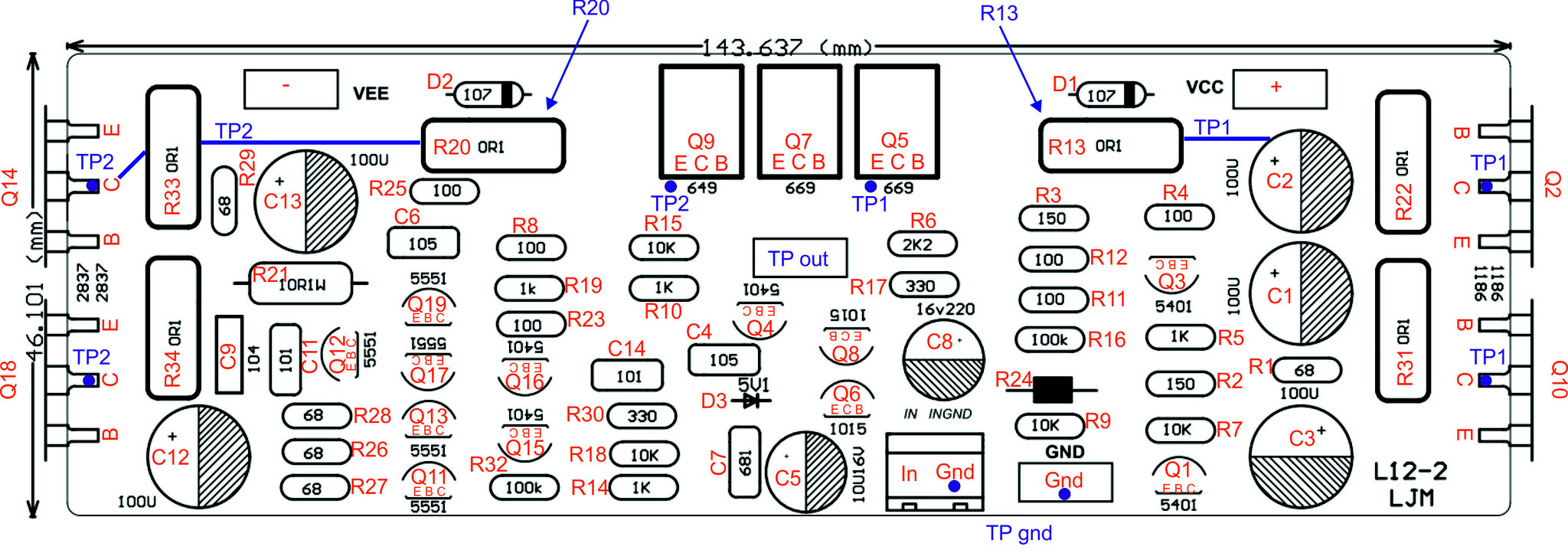
Lets start with some pictures and schematics.
Seemingly the amplifier is build on a long and thin PCB. With approximately 200mm of length, 50mm width and roundabout 30mm build-up height it is very well suited for mountage to the cooling fin sides of a casing or the backsides of active speakers. Immidiately the four potent power transistor from Sanken at the left and the right end of the PCB catch Your eye.
Those are so called ring-emitter or LAPT types, to which also the famous Sanken 2SA1216/2SC2922 in their MT-200 casings belong. In the early 90s the market was almost flooded with HighEnd amplifier that utilized these transistors, Burmester and Audio Research to name just two renowned brands.
The 2SA1186/2SC2837 are the smaller brethren of the 2SA1216/2SC2922 with a specced heat power loss of 100W and which are lower in capacitances and faster.
In the special connection as Sziklai-pairs, or complementary follower pairs (CFP) this plays a quite important role. A pair of the Sankens each form a Sziklai pair together with the -in the middle-of-the-PCB-positioned- driver transistors 2SD669/2SB649 (Q5/Q9, originally Hitachi/Renesas types, nowadays probabely from ISC). These transistors too belong to the best parts You can use here.
To find these and the Sanken combined to form Sziklai pairs in such a low-cost amplifier made me really curious.
Lets now move to the Input side:
The audio signal first passes a bandpass filter made up from R14/C7 and C5/R18 and reaches transistor Q6, that forms a differential amplifier input stage together with Q8. Its fed a constant current from the constant current source (CCS) Q1/Q3/R2. Q15 and Q16 cascode the differential stage. They keep the heat power loss low and provide for low input capacitance and high bandwidth. Towards the negative supply line follows a current mirror comprised of Q13/R26/Q11/R27.
It guarantees for good symmetry, high openloop gain and low sensitivity against disturbances on the supply rail (PSRR).
Q12 forms the voltage amplifying stage (VAS) that works on the CCS-connected Q4 as load. Between Q12 and Q4 we find the biasing network Q7/R10/R10/C6 that generates and regulates the bias voltage for the output stage.
It should be noted as specialty that the biasing transistor Q7 is thermally coupled to the driver transistors Q5 and Q9.
It must not(!) be thermally coupled to the power transistors Q2/Q10!Q14/Q18 as its done in a classic Darlington stage. Since the drivers vary less in temperature than the power transistors the bias current remains more stable.
The short and snappy feedback loop formed between the drivers and the power transistors then nicely stabilizes the power transistors bias current.
Due to the feedback action the CFP works more linear under large signal conditions, it can be pushed closer to the rails (efficiency) and requires only half the biasing voltage. The optimum bias current value is also roughly half the value of a Darlington, so that the CFP runs cooler.
Finally the always apparent differences between NPNs and PNPs tend to level out while they multiply with a Darlington.
There are only a couple of points to be kept in mind.
For one is the the CFP combined as ´super transistor´ slower and more prone to oscillation. The value of the collector resistor (R4/R25) should be as small as possible. The power transistors should be fast, low-capacitance types and the inductances and stray inductances of the layout and parts should be small.
Due to this its rather impossible to parallel connect more than two power transistors to the driver and damper-resistors connected to the power transistor bases might be required to prevent oscillation.
R15 und R17/C8 define the amplification factor. C8 reduces the DC-gain to 1. That spares the use of an actice DC-servo stage and functions flawlessly under all circumstances.
A 100pF Miller cap C12 is connected across Q12s collector-base junction as compensation cap. R30 and C14, located between the collectors of the input differential stage, also serve compensation means. They increase the openloop gain above a certain high frequency which improves stability (phase reserve).
At the output we find a Zobel network (also called Boucherot-network) that presents the amplifier a defined load at high frequencies.
Between the input stage cascode and the current mirror two diode connected transistors Q17 and Q18 function as protection circuitry.
The diodes D1 and D2 also serve protective purposes. A inductive load character can push energy back into the amlifiers output, resulting in a possible rise of the output voltage above the supply rails and possible destruction of the output transistors due to polarity reversal. The diodes ´catch away´ the overvoltage to their maximum forward voltage (hence the term ´catcher-diode´).
R32/D3/C4 supply for a constant bias of -5.1V at the bases of the input stage cascodes. The remaining parts are just a couple of caps for de-noising and local supply-rail decoupling.
There are even simpler build amplifiers around, but the additional effort put in here is just at the right points and guarantees a very good behaviour measurement-wise.
What becomes quickly obvious in praxis is the unconditionally stable performance into complex loads. My electrostats that show up to -86° of phase shift are a definite touchstone. Not only drives the amplifier even such specimen with utter stability, it also remains sonically sober. Many amp´s sound character shifts towards cold and hard long before the amp actually breaks into oscillation.
You can supply the amplifier over a quite large range of supply rail voltages.
A 2x24V ~ transformer will be good for 100W at 4Ohm, with a 2x32V~ trafo 100W at 8Ohms are possible. Due to the four power transistors it is even possible to connect two amps in a bridged mono configuration. Supplied from a 2x24V~ transformer one can drive around 150W into 8Ohm or close to 300W into 4Ohm.
This is quite an interesting alternative for active speaker concepts.
The Mids and Highs could be driven by single amplifiers while the power-hungry Bass can be driven from a bridged pair of amps. All can be supplied from one power supply from the same voltage rails. This keeps cost and effort low.
Die Nutzung der Texte, Bilder und Informationen auf dieser Webseite in Teil oder in Gänze bedarf meiner Zustimmung. The useage of the texts, pictures and information contained on this website in parts or in fullness requires my admittance.
Diese Webseite wurde mit Jimdo erstellt! Jetzt kostenlos registrieren auf https://de.jimdo.com


