L12-2 - modifications
As good as the L12-2 is, there remain some points where it can be improved or changed.
This applies to parts as well as the schematics.
But don´t worry, the changes are easy to do and reversible.
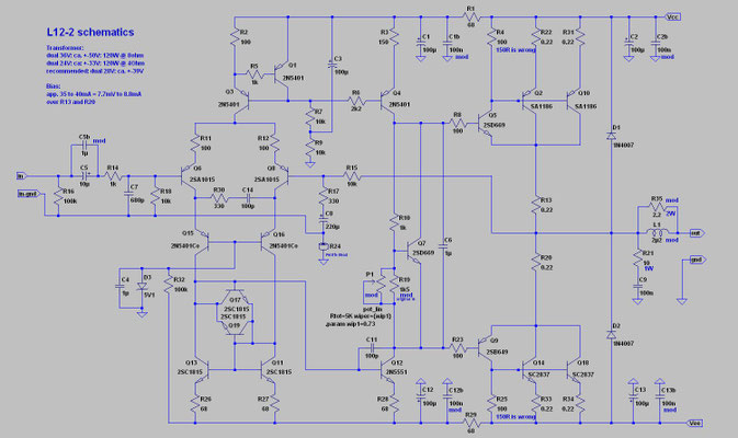
Lets take a look at the amplifier and its schematics again.
One will notice that the serial capacitors C5 in the input and C8 in the feedback path are aluminum electrolytics. Here You can connect small high-quality film caps in parallel, which is easy to do on the PCB solder side.
If the output of a source device is truely free from DC offset You can omit with C5 alltogether.
Parallel to the Lytics C1/C2/C12/C13, that decouple the supply rails, small film or ceramic X7R caps may be soldered, e.g. MKS2 of Wima from 100nF to 1µF, with a lead pitch of 5mm throughole or 1812 in SMD style.
Quite sensible is a modification to the bias network, since the Bias current values vary considerably from amplifier module to amplifier module.
Replace the 1kOhm R19 by a parallel connection of a 1.5kOhm resistor and a 5kOhm trim-potentiometer. This allows for a precise and consistent setting of the bias.
Though my amplifiers haven´t shown any signs of instability so far, the CFP output configuration is said to be more sensitive to capacitive loading than the Darlington.
Surprisingly it aren´t the larger capacitances in the µF range as electrostats present for example, but rather lower capacitances from cabling in the higher pF to several nF range that let an amplifier break into oscillation.
A LR-network R35/L1 with values of 8-10Ohms for R35 and 1µH-2µH for L1 is a good remedy.
Who likes can further beef up the high-current tracks on the PCB in that he solders copper wire on top or applys a thick layer of solder.
With this all the ´simple modifications´ are mentioned.
Additional modifications apply to the compensation networks and directly affect the signal related behaviour of the amplifier
These modifications should -as long as they have not been verified as working safely- be accompanied by measurements.
From my simulations a change from the simple Miller compensation to a 2-pole-compensation looks promising (just one cap and one resistor more).
While the openloop gain with Miller compensation drops by a rate of -6dB/oct above a low frequency break point, it stays high up to a few kHz with 2-pole-compensation, but then dropping by -12dB/oct.
With Miller compensation the feedback factor reduces already from low frequencies upwards and distortions rise accordingly. Typically You recognize a strong rise in the distortion plots above 1kHz. With the 2-pole compensation the feedback factor remains constantly high for much longer and as such the distortion rise occurs at considerably higher frequencies.
Now there are some renowned developers who argue that the frequency dependend rise of the distortions becomes audible as it rises over-proportional with the power level also. At least it might be an explanation why some amplifiers tend to sound brighter and harder with increasing volume level as the sonic balance shifts. If though the distortion plot remains constant over frequency up to roundabout 6kHz (as sensible limit), it´d raise evenly and inconspicious with power level.
Further testing of this matter could proove rewarding.
Meanwhile LJM has introduced own modifications and the actual revision is named L12-2 v.4.
It can be identififed by a new Logo in one of the corners of the PCB.
Its said to be a pic of a Panda but appears more like a facial of Home Simpson to me *lol*
Anyways, here´s an udpated schematic.
The differences to earlier revisions are:
C5: 33µF/25V lytic
C4, C6: 10µF lytic
C8: 1000µF lytic
D3: Zener 5V6
R24 (ferrite bead) omitted
R13, R20, R22, R31, R33, R34: 0R1
These infos are collected from the associated diyaudio thread.
As such I cannot guarantee the correctness even if they appear plausible.
Please let me know if you find errors in this schematic.
Die Nutzung der Texte, Bilder und Informationen auf dieser Webseite in Teil oder in Gänze bedarf meiner Zustimmung. The useage of the texts, pictures and information contained on this website in parts or in fullness requires my admittance.
Diese Webseite wurde mit Jimdo erstellt! Jetzt kostenlos registrieren auf https://de.jimdo.com


